

پاسخ : آموزش نکات مربوط به ساخت برد های چند لایه. یک بار برای همیشه!(شما هم کمک کنید )
نظر یکی از داکیومنت ها در رابطه با via in pad :
و...
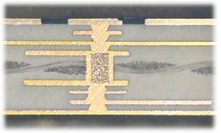
حالا فرض کنیم بیایم از ویا داخل پد استفاده کنیم . نتایج رو می تونید ببینید :

برای اینکه ویا ها رو توی پکیج بالا بین پد ها بچینیم باید سوراخ ویا ها کمتر از 0.05 میلیمتر و قطر ویا کمتر از 0.1 میلیمتر باشه !
با این وضعیت میشه سوراخکاری رو به صورت مکانیکی انجام داد و هزینه کاهش پیدا می کنه . اما باید سازنده این قابلیت رو داشته باشه که بتونه via in pad ها رو درست در بیاره. چند روش برای ساختشون هست و در نهایت اون چیزی که در میاد با ویا معمولی فرق می کنه چون باید داخل ویا پر شده باشه و البته هیچ ویا ای هم سر تا سری نباید باشه . ویا هایی که توی شکل می بینید بلیند هستند .
نظر یکی از داکیومنت ها در رابطه با via in pad :
[tt]Via in pad seems to be one of the hot topics these days. It's a bit of a tough one too. The smt guys
pretty much always say: "don't ever do it." However, with certain parts, the component
manufacturer strongly recommends it. You gotta love those mutually exclusive requirements.
Rather than just telling you "no, never", we re going to do our best to give a few guidelines on
how to do it properly.
We don't like it, but with some designs, if done properly, there can be a number of compelling
reasons for putting vias directly in the SMT pads for BGA and QFN packaged components.
It can make routing easier with big or fine pitch BGAs
It can allow really close placement of bypass capacitors
It can help with thermal management
It can help with grounding on high-frequency parts.[/tt]
و...
[tt]If your vias are left open, solder will tend to wick down
into the via hole. The larger the diameter, the worse the
wicking problem can be. You might end up without
enough solder left to secure the component, or even a
solder bump on the bottom side of the board which could
interfere with other components or lead to shorts.
If your vias are capped or partially filled, the caps might pop off due to thermal
expansion or out-gassing. Internal air bubbles can migrate up, leading to voids in your
solder joint.[/tt]
حالا فرض کنیم بیایم از ویا داخل پد استفاده کنیم . نتایج رو می تونید ببینید :
برای اینکه ویا ها رو توی پکیج بالا بین پد ها بچینیم باید سوراخ ویا ها کمتر از 0.05 میلیمتر و قطر ویا کمتر از 0.1 میلیمتر باشه !
با این وضعیت میشه سوراخکاری رو به صورت مکانیکی انجام داد و هزینه کاهش پیدا می کنه . اما باید سازنده این قابلیت رو داشته باشه که بتونه via in pad ها رو درست در بیاره. چند روش برای ساختشون هست و در نهایت اون چیزی که در میاد با ویا معمولی فرق می کنه چون باید داخل ویا پر شده باشه و البته هیچ ویا ای هم سر تا سری نباید باشه .
ویا هایی که توی شکل می بینید بلیند هستند .
 این موارد در مورد نویا هیچ ربطی به متالیزه کردن یا پوشش نهایی برد نداره ! اشتباه نگیرید!


 ) من هم برعکس کارای دیگم که عکسشون رو هیچ جا نمی گذارم این یکیرو قبل از ساخت 2 تا عکسش رو می گذارم شاید شما هم حوس کردید با لذت و رقبت بیشتری مطالب رو دنبال کنید . اون چیز میزای قرمز هم که نوشته فقط چون برد رو هنوز نساختم روی عکس ها نوشتم :redface:


 اونم نسخه ی پرتابلش! (که پر از باگه !)خود آلتیوم که از این کارا بلد نیست بکنه . خودم تک تک قطعات به صورت سه بعدی روی برد قرار دادم . خروجی های 3D MAX هم برای ساخت قالب ( که اصولا هنوز نتونستم برای یکی از برئم بسازم ) هم به قسنگی تمام میشه وارد طراحی کنید . البته بعضی مدل ها هم آمادشون هست یا از نرم افزار های دیگه میشه با واسطه وارد این محیط کرد .


دیدگاه